Understanding of Circuit Noise
To begin with…
Noise is one of the most important requirements in circuits design, espeially in signal-chain circuits, such as ADC, amplifier or band-gap reference. In this blog, I will clarify the noise from definition, calculation to some example, with adding some of my own understanding. This is also a summary-note of my study of this stage, and it may be a start of a series of blogs since I’m planning write a group of articles about some basic theories or circuit-design knowledges to make them more concrete for me. Back to this blog, most of them are from the books of Jacob Baker’s ‘CMOS Circuits Design, Layout and Simulation’ and Willy Sansen’s ‘Analog Design Essential’ .
Overview
The circuit noise actually includes many types, the quantisation noise, coupling noise and the inherent noise, but in this blog, I will mainly discuss the inherent noise which is resulted from the the discrete and random movement of charge. The nosie can corrupt the signal(imagine you are talking with your friend in the middle of a pub), and to characterise how much the signal is corrupted, and metrics Signal-to-Noise ratio(SNR) is proposed; to get the SNR, we must know the average power of the noise, so let’s start from some simple stuff.
Power and Energy
Starting from a simple sine-wave whose period is $T$ (Frequency is $f$), and the expression of it is $v(t)=V_P\ sin(2\pi f \cdot t)$, its the instantaneous power dissipated on a resistor $R$ will be:
\[P_{inst}(t)=\frac{v^2(t)}{R}=\frac{V_P ^2\ sin^2 (2\pi \cdot \frac{t}{T})}{R}.\]To get the average power dissipated on the resistor $R$, we must do integration, but how? If we integrate this sine-signal from $0$ to $ \infin $, the results also goes to infinity; this is no doubt and is useless for calculating the SNR. Back to the name “average power”, it looks like we need a averaging, like doing integration and “spreading” it evenly throughout the entire period of time (dividing it by the integrated time).
Yes, for sine-wave which is periodical, we actually only need to focus on one cycle; based on this, the average power dissipated could be gotten(the integration is the instataneous power and spreading it throughout the period T):
\[Average\ power\ dissipated = \frac{1}{T} \int _0 ^T \frac{V_P ^2 sin^2(2\pi f \cdot t)}{R} \cdot dt;\]moving the resistor, the Mean-squared(MS) voltage could be gotten:
\[\bar{v^2}= \frac{1}{T} \int _0 ^T {V_P ^2 sin^2(2\pi f \cdot t)} \cdot dt\ ,\]with the units of volts squared. With this, the Root-mean-squared(RMS, “有效值” in Chinese) voltage of this sine wave signal is given:
\[\sqrt{\bar{v^2}} = V_{RMS}=\sqrt{\frac{1}{T} \int _0 ^T {V_P ^2 sin^2(2\pi f \cdot t)} \cdot dt\ }=\frac{V_P}{\sqrt{2}},\]with the units of voltage. We can also say that when $V_{RMS}=V_{DC}$, the power dissipated by the resistor with either a sinusoidal or DC source is the same.
In addition to this, when performing noise analysis, for example, check the total noise powre at the output form different source, the MS value is normally summed up, rather than the RMS value since the MS value is actually something that represents the power of each noise source (Summing power rather than summing voltage).
Power Spectral Density(PSD)
The PSD can be understood unless we know the principles of Spectral Analyser(SA), so let’s start from it. The figure below is the basic structure of a SA, including a multiplier, a oscillator(OSA), a bandpass filter and a power meter.
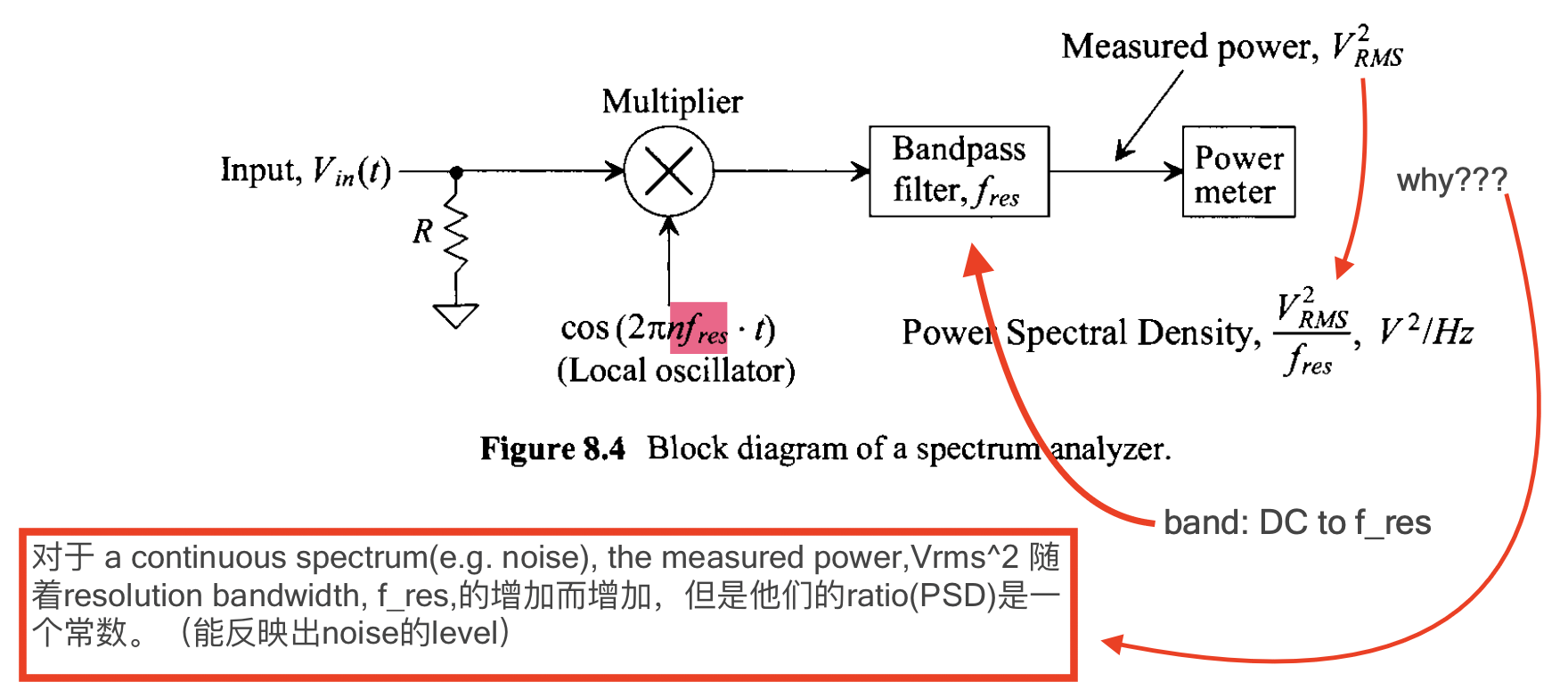
Basically, the OSC scans different fundamental frequencies with a step size of $f_{res}$ (as well as the resolution of the SA) and times the group of frequencies with the input frequency one by one (not at the same time);
The bandpass filter whose bandwidth is from $0$ to $f_{res}$ filters the products and then the power meter measures the power of its output.
But why do this system can know the spectral information of the input? It will be clear if we look the example below.
Example
Input: $V_{in}(t) = 1+ sin(2 \pi \cdot 4.05kHz \cdot t)$ , unit $V$
OSC signal: $V_{osc}(t)=cos(2\pi \cdot nf_{res} \cdot t)$ , unit $V$
Measured bandwidth: $0$ ~ $10\ kHz$ ($f_{stop}$)
Resolution: $f_{res}=100\ Hz$, the n will from 0 to 100
-
$n=0$
- $V_{osc}(t)=1$ (DC) The signal applied to the power meter is $(1V)^2$ ;
- MS: = $1/2\ V^2$ RMS: = $1/\sqrt{2} \ V_{RMS}$ Power: =$1/(2R) = V_{RMS}^2 / R$ ($R$ is the input resistance of SA)
- PSD: = $Power/ f_{res} = 1/(2\cdot R\cdot f_{res})$ with the units of $W/Hz$ or $Joules$ VSD: = $V_{RMS} / \sqrt{f_{res}}$, with the units of $V/\sqrt{Hz}$
Normally, for PSD, the $R$ is the thing we want to eliminate from the calculation, so we use the PSD like: $V_{RMS}^2 / f_{res}$, with the units of $V^2 / Hz$.
- $n=1$
-
The output of the multiplier is:
$ =cos(2\pi \cdot 100 \cdot t) \cdot (1+sin[2\pi \cdot 4.05kHz \cdot t ]) $ Volts
$ = cos(2\pi \cdot 100 \cdot t) + \frac{1}{2} { sin[2\pi(3.95k)t]+sin[2\pi(4.15k)t]} $ Volts
-
All the components can not pass the filter until $n=40$.
-
- $n=40$
- The output of the multiplier is: $ = cos(2\pi \cdot 4k \cdot t) + \frac{1}{2} { sin[2\pi(50)t]+sin[2\pi(8.05k)t]} $ Volts
- The second term can pass the filter, and the measured amplitude at the power meter is $0.5\ V$.
- $n=41$
- The output of the multiplier is: $ = cos(2\pi \cdot 4.1k \cdot t) + \frac{1}{2} { sin[2\pi(-50)t]+sin[2\pi(8.15k)t]} $ Volts
- The second term can pass the filter (the phase is inverting), and the measured amplitude at the power meter is $0.5\ V$.
$n=40$ and $n=41$ are actually the adjacent points of the input frequency component ($4.05kHz,\ n= 40.5$), and the sum of them are the amplitude of the input frequency component($4.05kHz$).
This phenomenon in my opinion can be understood like the emergy of the input is spread through the adjacent points?(but it’s wired why its amplitude equals to the sum of amplitude of adjacent points)
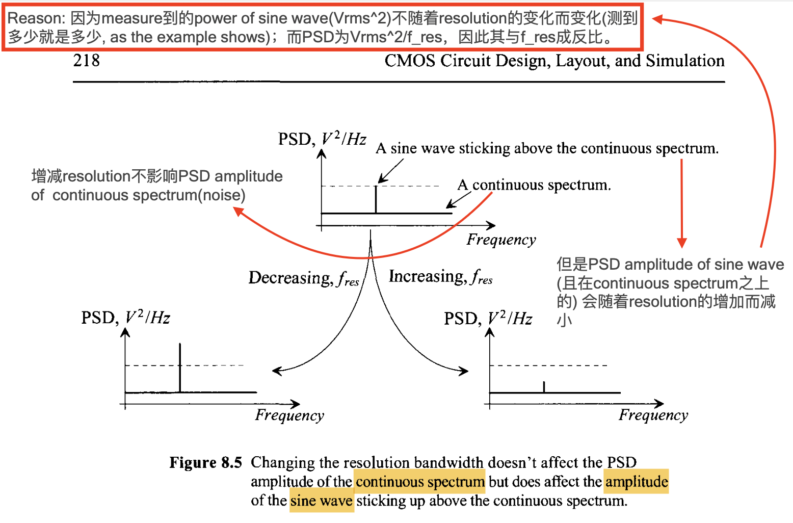
The reason why we use PSD rather than Power: There is some properties during the analysis of SA(also shown in the figure):
- when measuring the singal with continuous spectrum (like noise), increasing the $f_{res}$ will increase the power measured with a same factor, and the ratio between them, $V_{RMS}^2/f_{res}$, is constant, which is actually the definition of PSD.
- measuring the signal without continuous spectrum (like sine wave, only have discrete components) is different, the power measured at the certain frequencies is constant no matter what $f_{res}$ is; however, for PSD, increasing the $f_{res}$ makes the ratio smaller, shown in the figure(denominator increases).
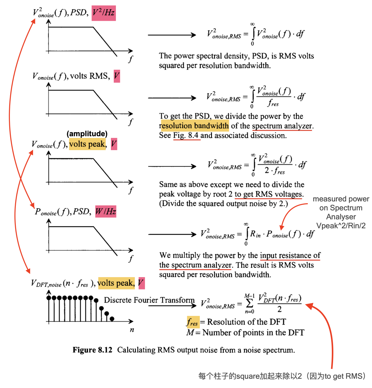
Summary: calculating $V_{noise,RMS}$ from a Spectrum
Most of time, we can get some information of the noise spectrum with different types… and here are the ways we use them to calculate the RMS value.
Circuit Noise
Before diving in to the specific circuits, defining and modelling the circuit noise at system-level is more intuitive, especially understanding the input-referred noise and so on.
Calculating and Modeling the Circuit Noise
RMS of circuit noise
The calculation of RMS value of the circuit noise is different from that of a periodical signal; for a periodical signal, the integration is done within a single period and divide the integration with its period. However, for the calculation of RMS of the noise, it is:
\[V_{RMS} = \sqrt{\int_{f_L}^{f_H}{ V^2_{noise}(f)\cdot df }}\ \ \ Volts,\]where $f_L$ and $f_H$ are the lower limit and higher limit of the bandwidth of interest; $V^2_{noise}(f)$ is the noise’s PSD(units, $V^2/Hz$).
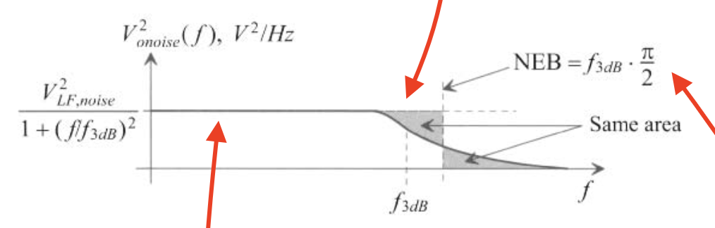
Noise equivalent bandwidth(NEB)
Normally, the noise is band-limited, so the bandwidth should be taken into account when calculating the RMS value of the noise. If the PSD of the noise is a signle-pole roll-off at the certain bandwidth $f_{-3dB}$, which is:
\[PSD(f) = \frac{V^2_{LF,noise}}{1+(f/f_{-3dB})^2},\]the RMS value of the noise will be:
\[V^2_{onoise, RMS} = \int_0^\infin PSD(f)\cdot df = V^2_{LF,noise} \cdot f_{-3dB}\cdot \frac{\pi}{2}=V^2_{LF,noise} \cdot NEB.\]From the calculation of the NEB, it can be easily concluded that the derivation is actually equivalent to a spreading the noise energy throughout the $ f_{-3dB}$ or finding a new upper limit of intertested bandwidth the “equivalent” noise PSD, like the figure below shows.
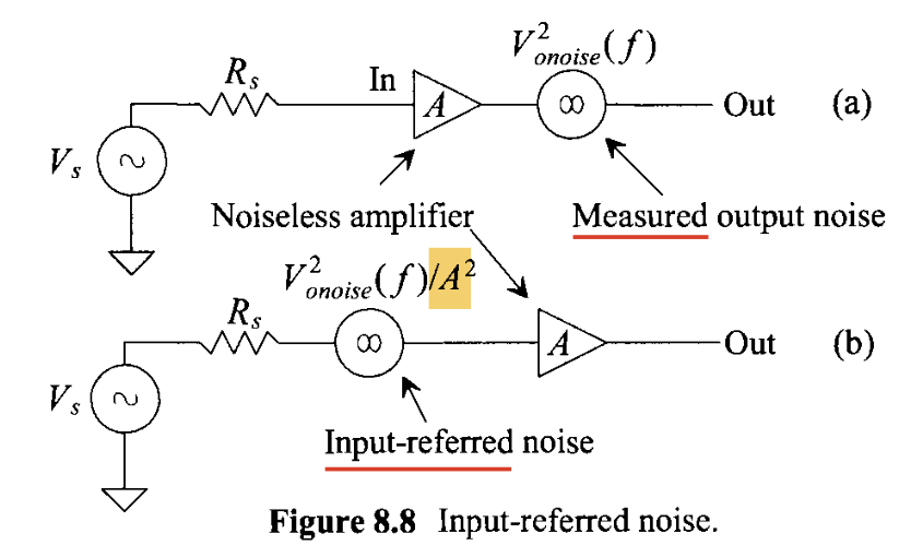
Input-referred Noise—definition
The input-referred noise is actually a thing that can not be measured directly. It is calculated by referring the measured output noise back to the input to compare with the input signal, shown in the Figure below. Therefore, it actually describes to what extent the input signal can be corrupted.
Input-referred Noise—modelling
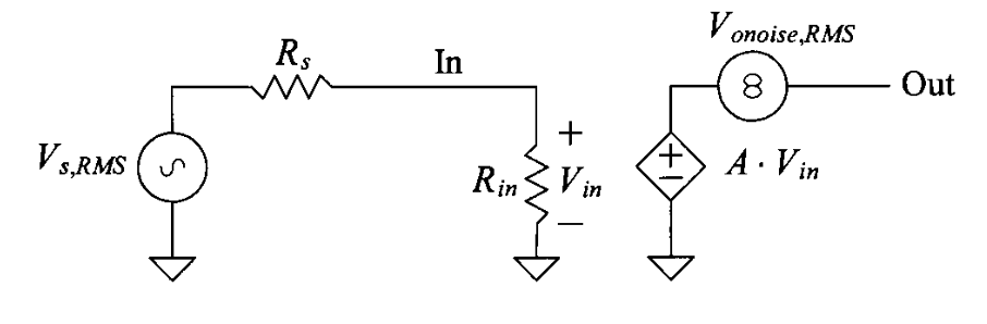
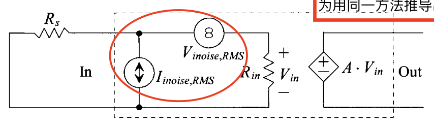
In order to handle different types of input sources (current/voltage) and make the input-referred noise independent of the source resistance($R_S$) ’s noise, a model for input-referred noise is proposed(not by me), which is shown in the figure below.
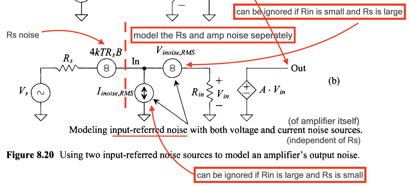
Like the figure above shows, the input-referred noise is modelled by a current source($I_{inoise,RMS}$) in parallel with the input resistance($R_{in}$) and a voltage source($V_{inoise,RMS}$) in series with the input resistance. The output noise can be calculated by:
\[V^2_{onoise,RMS}=4kTR_s\cdot B \cdot (\frac{AR_{in}}{R_s+R_{in}})^2 + I^2_{inoise,RMS}\cdot (\frac{AR_{in}R_{s}}{R_s+R_{in}})^2 + V^2_{inoise,RMS} (\frac{AR_{in}}{R_s+R_{in}})^2 \ ,\]where the first term is the noise generated from the source resistance $R_s$, and the calculation is simply done by the superposition theory.
This model can cover two scenarios we normally meet during the nose analysis:
- Scenario 1: voltage input source, $R_s « R_{in}$ . E.g. a voltage drives a voltage amplifier. In this case, the $I_{inoise,RMS}$ can be ignored, since the $V_{in}$ it generates is attenuated by the $R_s$.
- Scenario 2: current input source, $R_{in} « R_{s}$ . E.g. a voltage drives a trans-impedance amplifier (TIA). In this case, the $V_{inoise,RMS}$ can be ignored, since most of the voltage drops on the source resistance $R_s$.
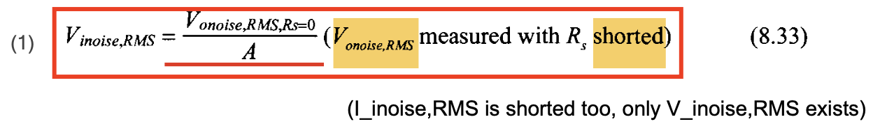
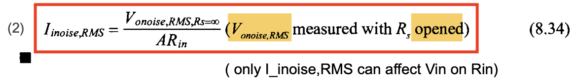
The way to determine the $V_{inoise,RMS}$ and $I_{inoise,RMS}$ is also straightforward, very similar to the determination of the input impedance of a system, shown as below:
Signal-to-Noise Ratio(SNR)
A very common metrics in the signal chain circuits, like the amplifiers or ADCs, and can be calculated by:
\[SNR=10\ log \frac{P_s}{P_{noise}}=20\ log\ \frac{V_{s,RMS}}{V_{noise,RMS}}\]In addition, for a system, it will also has two metrics called $SNR_{in}$ and $SNR_{out}$; for $SNR_{in}$, it only considers the noise of signal source, or in other words, the qulity of the input signal to the system; while for the $SNR_{out}$, it is a metric to evaluate the qulity of the system output.
For the system shown above, those two metrics can be calculated by:
\[SNR_{in}=\frac{V^2_{s,RMS}\ \cdot [\frac{R_{in}}{R_{in} + R_s}]^2}{4kTR_s B \ \cdot [\frac{R_{in}}{R_{in} + R_s}]^2} = \frac{V^2_{s,RMS}}{4kTR_s B}\] \[SNR_{out} = \frac{V^2_{s,RMS}\ \cdot [\frac{R_{in}}{R_{in} + R_s}]^2 \ \cdot A^2}{V^2_{onoise,RMS}}\]Noise Figure (NF)
For a system, $SNR_{in}$ and $SNR_{out}$ can be different, and for a phasical system, the $SNR_{in}$ is normally larger than $SNR_{out}$ since the system will always have noise and corrupt the signal. Therefore, a new metrics is propose, the NF, to evaluate how “noisy” the system is, and the way it is calculated is:
\[NF=10\ log\frac{SNR_{in}}{SNR_{out}} = 10\ log(SNR_{in}) - 10\ log(SNR_{out}) = 10\ log(F),\]where $F$ is another metric called Noise Factor.
Types of Circuit Noise
Thermal Noise
One of the most common type of noise in circuits analysis, which is caused by random motion of electrons due to thermal effects(leading to lattice vibrations). For a resistor, its thermal noise can be modelled by two ways, a current source or a voltage source, shown as below:
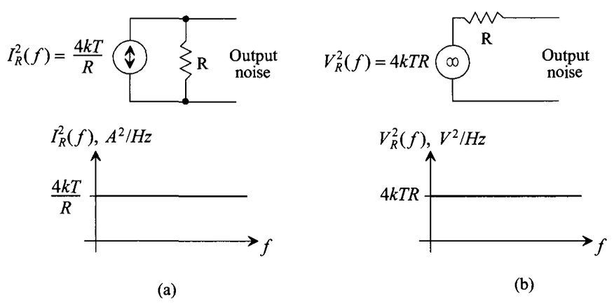
where $I^2_R(f)$ and $V^2_R(f)$ are the PSD of the thermal noise, with current and voltage forms respectively. In addition, inside the equation, $k$ stands for Boltzmann’s constant ($13.8 \times 10^{-24} J/K$), and $T$ is the temperature in $K$, so the unit of $kT$ is Joules .
As you can see, the PSD of the thermal noise is flat from zero to infinity and direct proportional to the resistance, what a hardworking noise source! Then what the output noise of a low-pass filter would be?
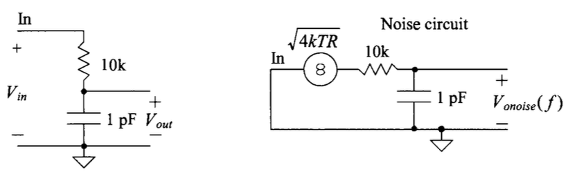
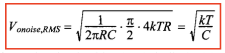
We already have the answer: $kT/C$ noise! referring to the definition of NEB, the noise of this resistor will be filtered out and interestingly, the RMS value of this system(shown as below) has nothing to do with the value of the resistor. Also, please stick this thing into your mind: $kT/C$ is not the PSD! it’s squre of RMS!
This is a very useful conclusion for filter design: we can not increase the value of resistance without thinking of the noise.
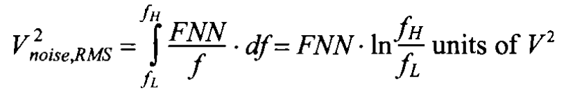
Fliker Noise(pink noise), 1/f noise
Another common type of noise that needs to be considered in circuit design, especially the ciruits with transistors. Fliker is a low-frequency noise that can significantly corrupt your SNR, and its PSD is inversely proportional to the frequency(1/f).
Fliker is normally modeled by
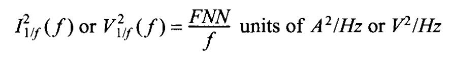
where $FNN$ is the fliker noise numerator, and the RMS value of Fliker would be:
Shot Noise
This is a type of noise that is not paid much attention to attention to since it mainly happens in short channel transistors and results from the discrete movement of charge across a potential barrier(depletion region). In addition, it is not easy to precisely describe shot noise by PSD, which is empirically given by:
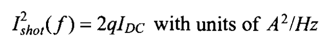
;from the equation, it can be seen that the shot noise is modeled with a white noise PSD and a interesting property of it and a main difference of it to the thermal noise is: the presents of shot noise rely on the current flowing through the resistor. To be academically, as Jacob Baker says, the present of shot noise must have both a potential barrier and a current flowing, and also movement across the barrier is random and in one direction.
Discussion
Correlation
Startig with a simple example shown in the figure below, what’s the power dissipated on the resistor if the RMS value of $v_1(t)$ and $v_2(t)$ is $V_{1RMS}$ and $V_{2RMS}$ respectively. This question looks quite straightforward; why? Since the RMS value of a signal is derived from the power dissipation on the resistor. In addition, when we calculated the output noise of a circuits, the square of RMS values of different sources are added. Therefore, the answer shoud be $P_{AVG} = (V_{1RMS}^2 + V_{2RMS}^2)/R$ ?
Wrong! This answer is only right when $v_1(t)$ and $v_2(t)$ are non-correlated. Then, what is “correlated” or “correlation”?
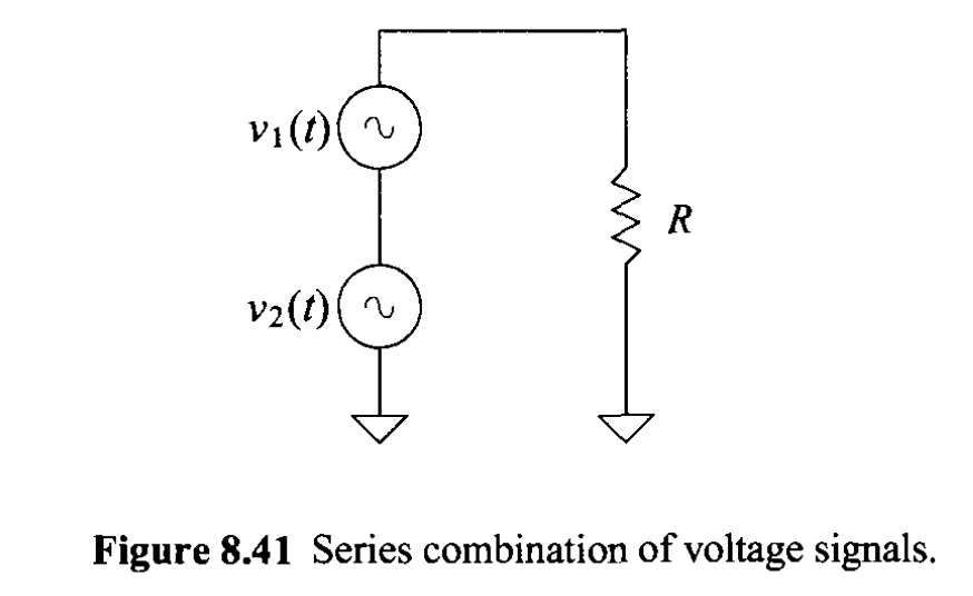
Let’s go back to the definition of power and transient power on the resistor which is:
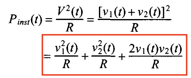
Looking at the last term, which has the product, it is tricky since this thing is actually a product of two transient waveforms. Let’s think about two special cases:
-
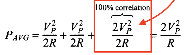
$v_1(t) = v_2(t)=V_P \cdot sin2\pi f \cdot t$ In this scenario, a combined signal with a peak amplitude of $2\ V_P$ will be applied on the resistor, and the overall power dissipated on the resistor is:
-
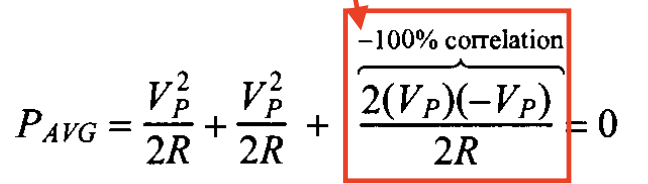
$v_1(t) = -v_2(t)=V_P \cdot sin2\pi f \cdot t$ It is easy that the combination of two is zero, means they cancel each other, so the overall power is:
In addition, it will have some combination between these two, for example, two signals with same frequency but have a $\pi /2$ phase difference or with same frequency but different amplitudes.
To describe the correlation between two signals, a parameter $C$ is created, and $-1<=C <=1$ if $C=0$, no correlation between, if $C=-1$, $-100%$ correlation between, and if $C=1$, $100%$ correlation between.
Correlation of Input-referred Noise Source
Remember the model of Input-referred noise model? The noise of an amplifier is modelled by an input-referred current source and voltage source, and the calculation of output noise is given by (already shown and discussed above):
\[V^2_{onoise,RMS}=4kTR_s\cdot B \cdot (\frac{AR_{in}}{R_s+R_{in}})^2 + I^2_{inoise,RMS}\cdot (\frac{AR_{in}R_{s}}{R_s+R_{in}})^2 + V^2_{inoise,RMS} (\frac{AR_{in}}{R_s+R_{in}})^2 \ .\]Paying attention to the last two terms, this equation makes sense when there is no correlation between $V_{inoise,RMS}$ and $I_{inoise,RMS}$, why? Since when we consider the actual input of the amplifier, $V_{in}$, it should be (ignoring the thermal noise of $R_s$ ) the superposition of those two (I paste the circuit as below to clarify), right? Therefore, the manner of the output noise should be the square of the superposition, rather than the summation of squares (i.e. square after summation).
Based on those, we can rewire the output noise (still ignoring the thermal noise of $R_s$ :
\[V^2_{onoise,RMS}=\left( \frac{AR_{in}}{R_s + R_{in}} \right)^2 [V_{inoise,RMS}+I_{inoise,RMS}\cdot R_s]^2 \ \ \ \ \ \ \ \ \ \ \ \ \ \ \ \ \ \ \ \ \ \ \ \ \ \ \ \ \ \ \ \ \ \ \ \ \ \ \ \ \ \ \ \ \ \ \ \ \ \ \ \ \ \ \ \ \ \ \ \ \ \ \ \ \ \ \ \ \ \\ = \left( \frac{AR_{in}}{R_s + R_{in}} \right)^2 [V_{inoise,RMS}^2 + I_{inoise,RMS}^2 \cdot R_s + 2C \cdot V_{inoise,RMS} \cdot I_{inoise,RMS}],\]it can be seen that if $C=0$ , this equation will be equivalent to the one above.
Then, what about the correlation between them in the practical circuits? Is $C=0$ making sense? The answer is of course no, since inside the model, these two ($V_{inoise,RMS}$ and $I_{inoise,RMS}$) are derived from same noise mechanism. However, as Baker’s book saying, to use the model, “we generally assume no correlation ($C=0$) between $V_{inoise,RMS}$ and $I_{inoise,RMS}$.”.
I guess this assumption is for simplicity of calculation and analysis, although I‘m still kind of confused about it.
Complex Input Impedance
This may be a point that is negligible since it too basic, but there are still some points are worthy to emphasise.
First thing first, is taking the magnitude before squaring, what that mean? Imagine, we have a amplifier and a voltage source with a source impedance $R_s$ as the amplifier’s input, and in addition, the input imedance is $Z_{in}$ (no longer $R_{in}$); then, the actual input singal of the amplifier is:
\[V_{in} = V_s \cdot \frac{|Z_{in}|}{|R_s + Z_{in}|}\ \ or\ \ V_{in}^2 = V_s^2 \cdot \frac{|Z_{in}^2|}{|R_s + Z_{in}|^2}.\]Here is the point, how to calculate the denominator? Do $a^2 +b^2 +2ab$ ? No! that’s what high school students may did. The correct way is treat it as a vector(it is actually) and calculate the magnitude. For example, if $Z_{in} = 1/j \omega C_{in}$, the correct way should be:
\[|R_{s}+Z_{in}|^2 = \left( \sqrt{R_s^2 + (1/\omega C_{in})} \right)^2 = R_s^2 + (1/\omega C_{in})^2.\]Second thing is Optimum Source Resistance. It is all known that to get both maximum power transfer and the best noise performance, the input resistance should be matched with the source resistance, like:
\[R_{s,opt} = R_{in}.\]However, when one of them is complex, for example the input impedance of the amplifier(actually true for most of the time), the equation above would be:
\[R_{s,opt} = |Z_{in}| = |R_{in} + jX_{in}| = \sqrt{R_{in}^2 + X_{in}^2},\]then, is it the optimum source resistance? Well, yes and no. “It only YES without regard for maximum power transfer” ( from Baker’s book. so does it mean best noise performance? better to have a derivation here).
The theory is: “the requirement for maximum power transfer is making the source impedance the complex conjugate of the load impedance.” Therefore, as you can see, if the source resistance is real, this requirement will be impossible to be met.
For radio-frequency circuits, they usually use the impedance transformation circuits to gain both maximum power transfer and nosie performance.
Noise and Feedback
Normally the amplifiers are used in a feedback loop, and the places that the noise is introduced in can make a lot of difference, so discussing different scenarios is necessary. A very common single feedback loop is shown in the figure below, where $A$ is open-loop gain and $\beta$ feedback ratio, and there are four possible places that the noise can be introduced inside the feedback loop.
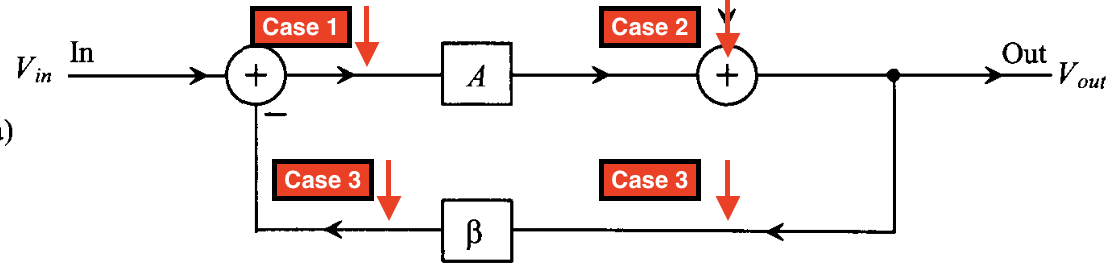
Assuming the introduced noise is $V_{noise}$, for the noise it represents to the output(or it transfer function to the output), it can be easily derived:
-
Case 1: the noise is amplified by closed-loop gain
\[V_{out} = \frac{A}{1+\beta A} (V_{in}+V_{noise,1})\] -
Case 2: the noise is shaped by loop-gain (Noise-shaping)
\[V_{out} = \frac{A}{1+\beta A} \cdot V_{in} + \frac{1}{1+\beta A} \cdot V_{noise,2}\] -
Case 3: equivalent to the Case 1, just a phase inverting (and normally we do not care about the phase of noise)
\[V_{out} = \frac{A}{1+\beta A} (V_{in}-V_{noise,3})\] -
Case 4: the noise is directly superpositioned at the output.
\[V_{out} = \frac{A}{1+\beta A} (V_{in}- \beta \cdot V_{noise,4}) \approx \frac{1}{\beta} V_{in} - V_{noise,4}\]
These are just some general conclusions, which are just give us a brief impression, and for the specific circuits, we need specific analysis.
Another about these four cases that should be pointed out is: for the Case 1 and Case 2, they are some time equivalent. Why? Because for some circuits (for example, the closed-loop op-amp), the noise in Case 1 is the input-referred noise of Case 2 (in other words, they are correlated), which means:
\[V_{noise,2} = A \cdot V_{noise,1},\]applying this into the equation of Case 2, it can be found that this equation turns into the equation of Case 1. Therefore, in this case, it can be concluded that the feedback doesn’t affect the circuit’s noise performance.
This conclusion can also be applied to the nosie introduced at the places like Case 3 and Case 4.
It is worthy to compare this with some special case, for example, the delta-sigma modulator or some circuits implemented Noise-shaping technique, for these cases, the noise introduced at the places like Case 2 can be suppressed by the feedback loop.
Copyright Statement
This article is an Original Work of Bohao, if reprinted, please indicate the source: http:/merenguelee.github.io/2025/02/24/Understnading-of-circuit-noise/