Loop Design of PLLs
Reference:
-
[Analysis and Design of Phase-Locked Loops] — Prof. Shen-Iuan Liu
-
[https://en.wikipedia.org/wiki/Q_factor]
-
[https://blog.csdn.net/luohuo9844/article/details/133749833]
Overview
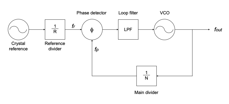
The phase-locked loop(PLL) normally contains frequency dividers, a phase/frequency detector(PFD), a loop filter and a voltage-controlled oscillator(VCO), as shown in the figure below. A good way to understand this loop is to analogy with the delta-sigma modulator(DSM), DSM is in the voltage domain while PLL works in the frequency domain.
The items in the loop provide a large gain to implement something like “Noise-shaping”, and this large gain is mainly provided by the VCO, which transfer in the frequency domain is $K_{VCO}/s$, like an integrator. This is more understandable when the linear model of the PLL is constructed, as shown in the figure below.
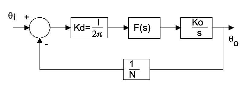
Ps: Because a good way to simulate the loop stability of PLL “directly” doesn’t exist, this model will be used again when the loop stability of the PLL needs to be verified.
Third Order PLL
Open- Loop Response
Normally, the $3{rd}$ order PLL has a $2{nd}$ order loop filter, corresponding to the $F(s)$ on the system diagram, and the most common $2_{nd}$ The order loop filter consists of one resistor and two capacitors, as shown below.
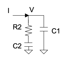
One thing that needs to be focused on is that the input of the loop filter is actually current rather than voltage because normally the output of PFD is converted to the current by a Charge Pump(CP), and the transfer function of the loop filter can be derived as below:
\[F(s) = \frac{V}{I}=(R_2+ \frac{1}{sC_2}) || \frac{1}{sC_1}=\frac{1}{C_1 + C_2} \frac{s \tau _2+1}{s(s \tau_1 + 1)} \ ,\]where $\tau_1 =R _2 {(C_1 C_2)}/{(C_1 + C_2)}$ , and $\tau_2 = R_2 C_2$. From the $F(s)$, a zero and two poles can be seen:
\[\omega_Z = -\tau_2 ^{-1} = -\frac{1}{R_2C_2},\ \omega_{p0} = 0,\ \omega_{p} = -\tau_1 ^{-1} = -\frac{C_1 + C_2}{R_2(C_1 C_2)} = \omega_Z(1+\frac{C_2}{C_1})\]Based on the system diagram and the derivation above, the loop gain of the PLL is given by:
\[G(s)=\frac{K_d K_{vco} F(s)}{sN}\ ,\]where $K_d$ is the gain of the PFD and CP.
Considering the inverted phase, the loop gain would be:
\[-G(s)|{s=j\omega} = \frac{ -K_d K_{vco}(1+j\omega \tau_2)}{\omega^2 C_1 N (1+j\omega \tau_1) } \cdot \frac{\tau_1}{\tau_2}\ ,\]and the phase of the transfer function is:
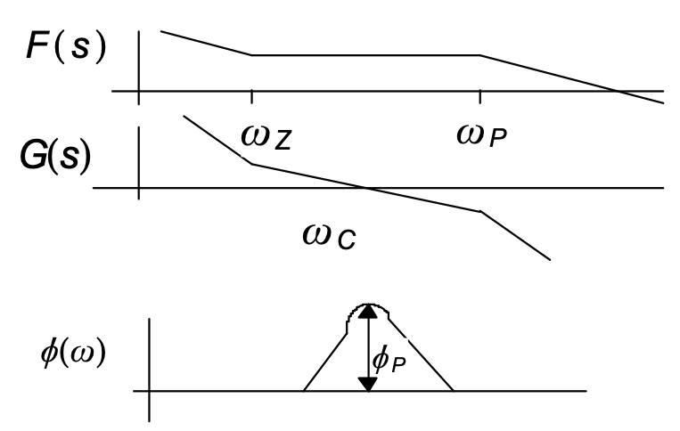
\[\phi(\omega) = tan^{-1}(\omega \tau_2)-tan^{-1}(\omega \tau_1) + 180^o, \\ \phi(f) = tan^{-1}(\frac{f}{f_Z})-tan^{-1}(\frac{f}{f_{p}})+180^o.\]Therefore, the maximum phase margin of this system setup can be calculated by letting $(d \phi(\omega)/d \omega) = 0$ at $\omega_C$, where $\omega_C$ is the unity gain-bandwidth of the open-loop gain. In this case, the $\omega_C$ and the maximum phase margin can be obtained:
\[\omega_C = \frac{1}{\sqrt{\tau_1 \tau_2}}, \\ \phi_p = tan^{-1}(\omega \tau_2)-tan^{-1}(\omega \tau_1),\]and this means the phase margin is mainly determined by the zero and the second pole, and the $\omega_C$ is at the “middle” of $\omega_Z$ and $\omega_{p2}$ (Geometric mean), so, the bode plot would be something like the figure below.
In addition, the unity-gain-bandwidth(UGB) can be calculated from the open-loop gain by making the $G(s)=1$ at $\omega_C$ :
\[G(\omega)\|{\omega =\omega_c}= K_d K_{vco} \frac{F(\omega) }{\omega\cdot N} = 1 \Rightarrow\ \omega_C = \frac{K_dK_vcoK_F}{N},\]where $K_F = \tau_2/(C_1 + C_2)$, and if the $C_2$ is way larger than $C_1$, the $K_F \approx R_2$. Therefore, the UGB would be:
\[\omega_C = \frac{K_d K_{vco}R_2}{N}.\]This important equation gives us a straightforward sense of the loop bandwidth.
Closed-Loop Response
With the equation of open-loop, for this system, the closed-loop response can be easily derived:
\[H(s) = \frac{N \cdot G(s)}{1+G(s)}=\frac{N\cdot K(s+\omega_Z)}{s^2(s/\omega_p +1)+ K(s+\omega_Z)},\]where $K=\omega_C = \frac{K_d K_{vco}K_F}{N}$, and for simplification, we define a factor $\gamma =\omega_C/\omega_Z = \omega_p/\omega_C$, which describes the “distance” between $\omega_Z$, $\omega_C$ and $\omega_p$. Therefore, the closed-loop response would be:
\[\Rightarrow H(s)=\frac{N\cdot (s+\omega_c / \gamma)}{s^3/\omega_p+s^2+\omega_c \cdot s+\omega_c^2/\gamma}= \frac{N\cdot \omega_c ^2 (s+\omega_c / \gamma)\cdot \gamma}{s^3+\omega_c\gamma \cdot s^2+\gamma\cdot \omega_c \cdot s+\omega_c^2}, \\ \Rightarrow \frac{H(s)}{N}= \frac{\omega_c}{\xi_2 -1}\left[ \frac{\xi_2}{s+\omega_c} - \frac{\xi_2+\omega_c}{s^2+s\cdot 2\cdot \xi_2\cdot\omega_c+\omega_c^2} \right],\]where the $\xi_2$ is the “Damping Ratio” of the system, and also $\xi_2 = (1/2Q)=(\gamma - 1)/2$, where $Q$ is the “Quality Factor”.
It can be observed that the second factor of the expression $H(s)/N$ is the normal expression of the second-order low-pass filter. Therefore, the theory of LTI system can also be applied to this scenario to help to understand.
If $Q<1/2$, the system is called an over-damped system, and for a closed-loop system, it will have a large PM, and in addition, if the $Q$ is too small, the system acts like a first-order system; If $Q>1/2$, the system will be underdamped, and has the risk of oscillating when the $Q$ is very small.
In the time domain, the $Q$ is related to the time-constant: $\tau = 1/\alpha = (2Q)/\omega_N$, where $\alpha$ represents the Attenuation Parameter. When the system’s $Q<1/2$, it has two conjugate poles that each have a real part of $-\alpha$.
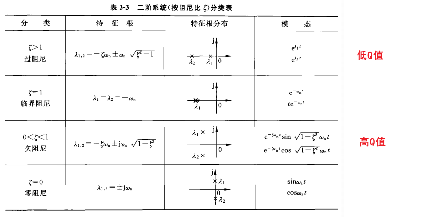
In addition, the factor $\gamma$ and $\xi_2$ can also decide the phase margin(PM) of the system, and the further they are from each other, the larger the PM will be, as shown in the table below.
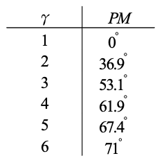
In conclusion, for the different parameters that have been discussed above, when $\gamma$ and $\xi$ is larger, $Q$ is smaller, the system is more stable.
Design Strategy
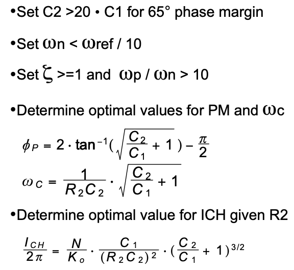
Having figured out the frequency response of the PLL loop, the conclusions should guide teh design of it. The figure below shows the design strategies given by the Prof. Shen-Iuan Liu which can be applied in normal design.
Reference Supr Attenuation
The reference spur is normally caused by the switching of the charge pump at teh reference rate, i.e. $F_{ref}$, and it will generate unwanted FM sidebands at the PLL output. The reference spur can be attended by adding an extra pole in the loop filter, as shown in the figure below.
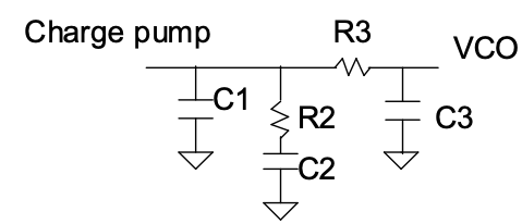
Since the addition of the pole can cause a decrease in PM, to minimise its effect, this pole is normally situated between $\omega_C$ and $\omega_p$. The added attenuation from the pole is given by:
\[Atten.=20log[(2 \pi F_{ref}\cdot \tau_3)^2+1],\]where $\tau_3 = R_3 \cdot C_3$. The attenuation of the reference spur is normally determined by the noise floor needed, so from a known attenuation, the location of the pole or the $\tau_3$ is:
\[\tau_3 = \sqrt{\frac{10^{Atten./20}-1}{(2\pi\cdot F_{ref})^2}},\]and the recommended value of $\tau_3$ is: $5\omega_C < \tau_3 ^{-1} < F_{ref}$, so this new added pole can affect the PM and even the $\omega_C$.
While for the design strategy of this pole, Prof. Liu suggested the approximation at first of the $\omega_C$ can be set up to $1/5 F_{ref}$.
Copyright Statement
This article is an Original Work of Bohao, if reprinted, please indicate the source: http:/merenguelee.github.io/2024/07/01/Loop-Design-of-PLLs/